APPARATUS OF SEMICONDUCTOR
DIODE
Diode are made from a P-type and N-type material. This material is joined to form a PN juction. This junction has polarity and can be forward or reverse biased.There is depletion region region where this PN junction forms.
A diode is a specialized electronic component with two electrodes called the anode and the cathode. Most diodes are made with semiconductor materials such as silicon, germanium, or selenium.
- A reverse-biased diode prevents current from going through it, due to the expanded depletion region. In actuality, a very small amount of current can and does go through a reverse-biased diode, called the leakage current, but it can be ignored for most purposes. The ability of a diode to withstand reverse-bias voltages is limited, as it is for any insulator. If the applied reverse-bias voltage becomes too great, the diode will experience a condition known as breakdown (Figure below), which is usually destructive. A diode's maximum reverse-bias voltage rating is known as the Peak Inverse Voltage, or PIV, and may be obtained from the manufacturer. Like forward voltage, the PIV rating of a diode varies with temperature, except that PIV increases with increased temperature and decreases as the diode becomes cooler -- exactly opposite that of forward voltage.


ZENER DIODE

The Zener , the current through a forward-biased PN junction is proportional to e raised to the power of the forward voltage drop. Because this is an exponential function, current rises quite rapidly for modest increases in voltage drop. Another way of considering this is to say that voltage dropped across a forward-biased diode changes little for large variations in diode current. In the circuit shown in Figure below (a), diode current is limited by the voltage of the power supply, the series resistor, and the diode's voltage drop, which as we know doesn't vary much from 0.7 volts. If the power supply voltage were to be increased, the resistor's voltage drop would increase almost the same amount, and the diode's voltage drop just a little. Conversely, a decrease in power supply voltage would result in an almost equal decrease in resistor voltage drop, with just a little decrease in diode voltage drop. In a word, we could summarize this behavior by saying that the diode is regulating the voltage drop at approximately 0.7 volts.

LED

A light-emitting diode (LED) is a two-lead semiconductor light. It is a basic PN junction diode, which emits light when activated. When a suitable voltage is applied to the leads, electrons are able to recombine with electron holes within the device, releasing energy in the form of proton. This effect is called electroluminescence, and the color of the light (corresponding to the energy of the photon) is determined by the energy band gap of the semiconductor.
An LED is often small in area (less than 1 mm2) and integrated optical components may be used to shape its radiation pattern.
Appearing as practical electronic components in 1962, the earliest LEDs emitted low-intensity infrared light. Infrared LEDs are still frequently used as transmitting elements in remote-control circuits, such as those in remote controls for a wide variety of consumer electronics. The first visible-light LEDs were also of low intensity, and limited to red. Modern LEDs are available across the visible,ultraviolet, and infrared wavelengths, with very high brightness.

In e;ectronics, an LED circuit is an electrical circuit used to power a light-emitting diode or LED. The circuit must provide enough current to light the LED at the required brightness, but must not allow so much current to flow as to damage the LED. The LED has a roughly constant voltage drop over a wide range of operating current, so a small increase in applied voltage will greatly increase current. Very simple circuits are used for low-power indicator LEDs. More complex circuits are required especially when driving high-power LEDs for illumination, where regulation of the current through the LED is required.
Transistor

Transistors can be regarded as a type of switch, as can many electronic components. They are used in a variety of circuits and you will find that it is rare that a circuit built in a school Technology Department does not contain at least one transistor. They are central to electronics and there are two main types; NPN and PNP. Most circuits tend to use NPN. There are hundreds of transistors which work at different voltages but all of them fall into these two categories.

The current flowing between emitter and collector of a transistor is much greater than that flowing between base and emitter. So a small base current is controlling the much larger emitter collector current. The ratio of the two currents, ICE / IBEis constant, provided that the collector emitter voltage VCE is constant. Therefore, if the base current rises, so does collector current.
This ratio is the CURRENT GAIN of the transistor and is given the symbol hfe. A fairly low gain transistor might have a current gain of 20 to 50, while a high gain type may have a gain of 300 to 800 or more. The spread of values of hfe for any given transistor is quite large, even in transistors of the same type and batch.
Input Characteristic.

The INPUT CHARACTERISTIC (right), a graph of base emitter current IBE against base emitter voltage VBE (IBE/VBE) shows the input CONDUCTANCE of the transistor. As conductance I / V is the reciprocal of RESISTANCE (V / I) this curve can be used to determine the input resistance of the transistor. The steepness of this particular curve when the VBE is above 1 volt shows that the input conductance is very high, and there is a large increase in current (in practice, usually enough to destroy the transistor!) for a very small increase in VBE. Therefore the input RESISTANCE must be low. Around 0.6 to 0.7 volts the graph curves shows that the input resistance of a transistor varies, according to the amount of base current flowing, and below about 0.5 volts base current ceases.
Output Characteristic.

Fig. 6.3 (right) shows the OUTPUT CHARACTERISTIC whose slope gives the value of output conductance (and by implication output resistance). The near horizontal parts of the graph lines show that a change in collector emitter voltage VCE has almost no effect on collector current in this region, just the effect to be expected if the transistor output had a large value resistor in series with it. Therefore the graph shows that the output resistance of the transistor is high.
The above characteristic graphs show that, for a silicon transistor with an input applied between base and emitter, and output taken between collector and emitter (a method of connection called common emitter mode) one would expect;
- • Low input resistance (from the input characteristic).
- • Fairly high gain (from the transfer characteristic).
- • High output resistance (from the output characteristic).
Transistor Circuits
Types of transistor
There are two types of standard transistors, NPN andPNP, with different circuit symbols. The letters refer to the layers of semiconductor material used to make the transistor. Most transistors used today are NPN because this is the easiest type to make from silicon. This page is mostly about NPN transistors and if you are new to electronics it is best to start by learning how to use these first.
The leads are labelled base (B), collector (C) andemitter (E).
These terms refer to the internal operation of a transistor but they are not much help in understanding how a transistor is used, so just treat them as labels!
These terms refer to the internal operation of a transistor but they are not much help in understanding how a transistor is used, so just treat them as labels!
A Darling pair is two transistors connected together to give a very high current gain.
In addition to standard (bipolar junction) transistors, there are field-effect transistors which are usually referred to as FETs. They have different circuit symbols and properties and they are not (yet) covered by this page.
Transistor currents
 The diagram shows the two current paths through a transistor. You can build this circuit with two standard 5mm red LEDs and any general purpose low power NPN transistor (BC108, BC182 or BC548 for example).
The small base current controls the larger collector current.
When the switch is closed a small current flows into the base (B) of the transistor. It is just enough to make LED B glow dimly. The transistor amplifies this small current to allow a larger current to flow through from its collector (C) to its emitter (E). This collector current is large enough to make LED C light brightly.
When the switch is open no base current flows, so the transistor switches off the collector current. Both LEDs are off.
A transistor amplifies current and can be used as a switch.
This arrangement where the emitter (E) is in the controlling circuit (base current) and in the controlled circuit (collector current) is called common emitter mode. It is the most widely used arrangement for transistors so it is the one to learn first.
Functional model of an NPN transistor
 The operation of a transistor is difficult to explain and understand in terms of its internal structure. It is more helpful to use this functional model:
- The base-emitter junction behaves like a diode.
- A base current IB flows only when the voltage VBE across the base-emitter junction is 0.7V or more.
- The small base current IB controls the large collector current Ic.
- Ic = hFE × IB (unless the transistor is full on and saturated)
hFE is the current gain (strictly the DC current gain), a typical value for hFE is 100 (it has no units because it is a ratio) - The collector-emitter resistance RCE is controlled by the base current IB:
- IB = 0 RCE = infinity transistor off
- IB small RCE reduced transistor partly on
- IB increased RCE = 0 transistor full on ('saturated')
- A resistor is often needed in series with the base connection to limit the base current IB and prevent the transistor being damaged.
- Transistors have a maximum collector current Ic rating.
- The current gain hFE can vary widely, even for transistors of the same type!
- A transistor that is full on (with RCE = 0) is said to be 'saturated'.
- When a transistor is saturated the collector-emitter voltage VCE is reduced to almost 0V.
- When a transistor is saturated the collector current Ic is determined by the supply voltage and the external resistance in the collector circuit, not by the transistor's current gain. As a result the ratio Ic/IB for a saturated transistor is less than the current gain hFE.
- The emitter current IE = Ic + IB, but Ic is much larger than IB, so roughly IE = Ic.
 |
 |
| Touch switch circuit |
Darlington pair
This is two transistors connected together so that the current amplified by the first is amplified further by the second transistor. The overall current gain is equal to the two individual gains multiplied together:
Darlington pair current gain, hFE = hFE1 × hFE2
(hFE1 and hFE2 are the gains of the individual transistors)
(hFE1 and hFE2 are the gains of the individual transistors)
This gives the Darlington pair a very high current gain, such as 10000, so that only a tiny base current is required to make the pair switch on.
A Darlington pair behaves like a single transistor with a very high current gain. It has three leads (B, C and E) which are equivalent to the leads of a standard individual transistor. To turn on there must be 0.7V across both the base-emitter junctions which are connected in series inside the Darlington pair, therefore it requires 1.4V to turn on.
Darlington pairs are available as complete packages but you can make up your own from two transistors; TR1 can be a low power type, but normally TR2 will need to be high power. The maximum collector current Ic(max) for the pair is the same as Ic(max) for TR2.
A Darlington pair is sufficiently sensitive to respond to the small current passed by your skin and it can be used to make a touch-switch as shown in the diagram. For this circuit which just lights an LED the two transistors can be any general purpose low power transistors. The 100k resistor protects the transistors if the contacts are linked with a piece of wire.
Using a transistor as a switch
 When a transistor is used as a switch it must be either OFF or fully ON. In the fully ON state the voltage VCE across the transistor is almost zero and the transistor is said to be saturated because it cannot pass any more collector current Ic. The output device switched by the transistor is usually called the 'load'.
The power developed in a switching transistor is very small:
- In the OFF state: power = Ic × VCE, but Ic = 0, so the power is zero.
- In the full ON state: power = Ic × VCE, but VCE = 0 (almost), so the power is very small.
For information about the operation of a transistor please see the functional modal above.

Protection diode
If the load is a motor, relay or solenoid (or any other device with a coil) a diode must be connected across the load to protect the transistor from the brief high voltage produced when the load is switched off. The diagram shows how a protection diode is connected 'backwards' across the load, in this case a relay coil.
Current flowing through a coil creates a magnetic field which collapses suddenly when the current is switched off. The sudden collapse of the magnetic field induces a brief high voltage across the coil which is very likely to damage transistors and ICs. The protection diode allows the induced voltage to drive a brief current through the coil (and diode) so the magnetic field dies away quickly rather than instantly. This prevents the induced voltage becoming high enough to cause damage to transistors and ICs.
SCR

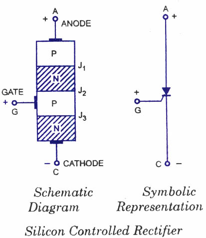
SCR is a 4 layer device (thyristor) which has three terminals, the anode, cathode and gate. Basically, the same as the SCR rectifier diode that has an element of control.
SCR is widely used as switching devices in power control applications. The basic structure of the SCR is as figure 4.1 and schematic symbol for SCR
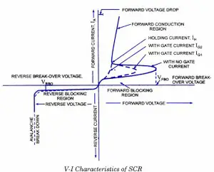
SCR characteristic curve is almost the same as normal diode characteristic curve unless there are some areas in the early stages that describe the current momentarily stuck.
During the lame front (VF), when IG = 0, no anode current (IA) are transmitted by the SCR was but little leakage current. Although VF is increased, IA still missing but a slight increase in leakage current. Flow at this level is called Flow Block Future (Forward Current Blocking).
With IG situation is still 0 and VF is further increased, will arrive at a voltage value where IA suddenly flows and rising rapidly. VF value at the time it was particularly cited the breakdown voltages Future (Forward breakover voltage, VBRF1). VBRF1 is when IG = 0.
If there IG (due to the positive voltage to the gate), which in the diagram labeled as IG2, breakdown voltages future events will occur much earlier (VBRF2). VBRF point can be lowered again by adding the IG. And so on until if IG adjusted to a high enough value, SCR will behave like a normal diode.
SCR when reverse biased (VR), SCR does not flow unless some leakage current or reverse current partitions. If VR is too high, it will get to the point inverse breakdown voltages. SCR act like ordinary diode in reverse bias condition.
TRIAC


Triac is a 5 layer device that can conduct current in both directions. Triac can also get triggered at the firing voltage is positive or negative.

Such as SCR, triac, also a three terminal device. The difference is that SCR flow in one direction only, but the triac bidirectional current flow.
Triac can be likened to two SCRs connected in parallel and opposite directions as shown in figure 4.5. Due to the anode of the SCR 1 SCR cathode is connected to 2, then the triac terminal labeled MT1 (main terminal 1) and MT2 (main terminal 2). Terminal triac gate still in use as terminal SCR 1 and SCR get 2 listed.
Triac characteristic curve is almost equal to the characteristic curve SCR except during reverse bias.
Reverse bias current, the arc is equal to the arc during the next lame but in opposite directions. Other features are similar to the characteristics of the characteristic curve of SCR. For example, the breakdown voltages will be reduced when the gate current increases.


Diac which is the same as triac not having a gate terminal. Therefore diac is a device labeled 2 terminal MT1 (main terminal 1) and MT2 (main terminal 2) only. Figure shows the schematic symbol for a diac.
-N2-P2-
Diac can also be likened to a diode which has 4 layers. Figure 4.9 shows the structure of the diac. The difference is that the diode current flow in one direction only, but diac flow in both directions. When MT1 positive, the current path is through the P2-P1-N1-N2. Conversely, if the MT2 positive, the current path is through 1N3.

curve Diac almost equal to the characteristic curve ripple except traits get there.
Unlike the SCR and triac,, diac will only operate when the voltage across it exceeds the breakdown voltage. Diak not have to get reduce the breakdown voltages.
Diac can conduct two-way. Thus the curve characteristic Diak during the current conflict is the same.
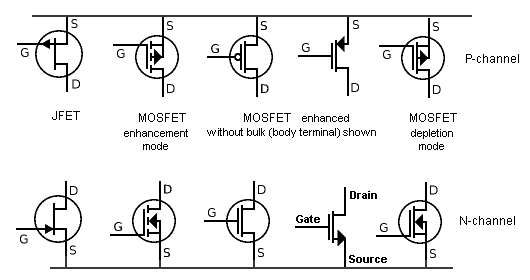
MOSFET

The metal–oxide–semiconductor field-effect transistor (MOSFET, MOS-FET, or MOS FET) is a type of transistor used for amplifying or switching electronic signals.
Although the MOSFET is a four-terminal device with source (S), gate (G), drain (D), and body (B) terminals, the body (or substrate) of the MOSFET is often connected to the source terminal, making it a three-terminal device like other field-effect transistor. Because these two terminals are normally connected to each other (short-circuited) internally, only three terminals appear in electrical diagrams. The MOSFET is by far the most common transistor in both digital and analog circuits, though the bipolar junction transistor was at one time much more common.
A cross section through an nMOSFET when the gate voltage VGSis below the threshold for making a conductive channel; there is little or no conduction between the terminals drain and source; the switch is off. When the gate is more positive, it attracts electrons, inducing an n-type conductive channel in the substrate below the oxide, which allows electrons to flow between the n-doped terminals; the switch is on.

Simulation result for formation of inversion channel (electron density) and attainment of threshold voltage (IV) in a nanowire MOSFET. Note that the threshold voltage for this device lies around 0.45 V.

Unijunction transistor:
Although a unijunction transistor is not a thyristor, this device can trigger larger thyristors with a pulse at base B1. Aunijunction transistor is composed of a bar of N-type silicon having a P-type connection in the middle. See Figure below(a). The connections at the ends of the bar are known as bases B1 and B2; the P-type mid-point is the emitter. With the emitter disconnected, the total resistance RBBO, a datasheet item, is the sum of RB1 and RB2 as shown in Figure below(b). RBBO ranges from 4-12kΩ for different device types. The intrinsic standoff ratio η is the ratio of RB1 to RBBO. It varies from 0.4 to 0.8 for different devices. The schematic symbol is Figure below(c)

The Unijunction emitter current vs voltage characteristic curve (Figure below(a) ) shows that as VE increases, current IE increases up IP at the peak point. Beyond the peak point, current increases as voltage decreases in the negative resistance region. The voltage reaches a minimum at the valley point. The resistance of RB1, the saturation resistance is lowest at the valley point.
IP and IV, are datasheet parameters; For a 2n2647, IP and IV are 2µA and 4mA, respectively. [AMS] VP is the voltage drop across RB1 plus a 0.7V diode drop; see Figure below(b). VV is estimated to be approximately 10% of VBB.

Unijunction transistor: (a) emitter characteristic curve, (b) model for VP .
The relaxation oscillator in Figure below is an application of the unijunction oscillator. RE charges CE until the peak point. The unijunction emitter terminal has no effect on the capacitor until this point is reached. Once the capacitor voltage, VE, reaches the peak voltage point VP, the lowered emitter-base1 E-B1 resistance quickly discharges the capacitor. Once the capacitor discharges below the valley point VV, the E-RB1 resistance reverts back to high resistance, and the capacitor is free to charge again.
No comments:
Post a Comment